

Welcome to China Hard Materials Parts. Thank you for visiting!
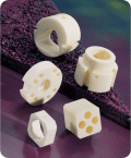
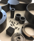
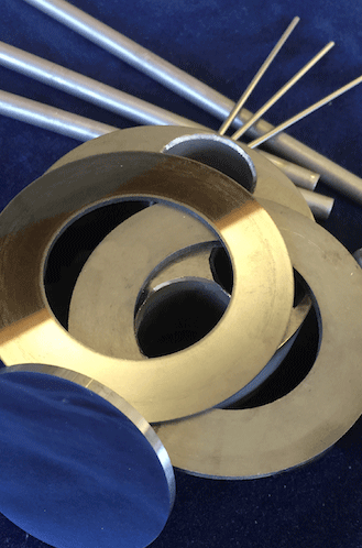
Since 1947, we have been a precision machining and polishing fabricator of parts from all technical ceramics, sapphire, glass and quartz. We machine these materials to very precise tolerances (many times measured in millionths of an inch) for dimension, flatness, wedge and roundness or cylindricity. Our customers typically have a critical application that requires extremely tight tolerances in ultra-hard materials. We also have the capability to grind and polish spherical radius parts in a variety of hard materials, both inside and outside diameters, to optical requirements.
Please feel free to navigate to other pages within our site to see more information on all of our high precision machining services, materials and capabilities. If you would like more information please click here to send a request, or visit our Frequently Asked Questions page.
Silicon is well known as a key component of electronic devices and also of solar cells. For these applications, the silicon must be purified from its initial form. Silicon is certainly a readily available raw material since it is actually the third most abundant element on Earth after only iron and oxygen, and is handy to isolate from common sand by reduction with coke in the presence of iron.
There are three basic forms of technical silicon available. They are monocrystalline, polycrystalline and amorphous. Most elemental silicon is produced as a ferrosilicon alloy and then refined to metallurgical grade purity. Only around 15% of is further refined to semiconductor purity. This purity is in the nine-9 level (99.9999999%) since electronic applications can’t function without such extreme purity.
Monocrystalline silicon is usually produced by the Czochralski process where a seed crystal is suspended in a molten bath of semiconductor grade silicon and slowly drawn while rotating under a protective atmosphere. The result is a long, round single crystal ingot that can weigh many hundreds of pounds. This crystal is then precision ground for diameter and then wire sawn into disks for further grinding for thickness and flatness and then polished to specification. The semiconductor industry processing benefits from ever larger diameter disks and has driven crystal growing development to at least 300 mm diameter and greater.
Monocrystalline silicon is intrinsically semiconducting, but can be doped by addition of other elements to make p-type or n-type silicon. The primary application is in production of discrete electronic components and integrated circuits. Another major application is for high-performance photovoltaic devices like solar cells.
Polycrystalline silicon is cast from molten silicon. It is also used for solar applications as it offers lower costs than the crystal grown material although it does not achieve as high purity or electronic efficiencies.
Because of years of high demand for precision wafer production, standard silicon wafers are readily available commercially and often produced in-house by semiconductor firms. Wafers are produced by highly automated systems and are therefore quite economical. Since 1947, China Hard Materials Parts has developed expertise and equipment to machine technical ceramics of all kinds to very precise dimension and unusual form. We are able to acquire single crystal silicon to desired specification in larger sizes from producers and then machine unique features precisely to our customer’s design. This has been useful for special R&D projects for our National Laboratories for example.
*Click on a Property to see a comparison of up to 10 materials
